-
PRODUCTS & SERVICESOptimized cooling solutions for modern data centersProducts & ServicesOptimized cooling solutions for modern data centers
-
CAPABILITIESAdvancing liquid cooling technologiesCapabilitiesAdvancing liquid cooling technologies
-
TechnologiesLiquid Cooling InnovationTechnologiesLiquid Cooling Innovation
-
RESOURCESLatest News & InformationResourcesLatest News & Information
-
ABOUTOur history, leadership and ownershipAboutOur history, leadership and ownership
-
CONTACTFacility locations and global operational footprint



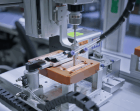



What Is the Best Type of Electronic Boards from China?
Choosing the best Electronic Boards from China requires more than comparing unit prices. The right choice depends on circuit density, operating conditions, volume, and compliance needs.
Prismark’s 2024 PCB industry analysis identifies China as the world’s largest printed circuit board production base. This scale supports broad capabilities, from standard multilayer boards to HDI, rigid-flex, and aluminum-backed designs. However, production scale does not guarantee consistent quality. IPC’s 2024 Global Sentiment of the Electronics Industry report highlights continuing pressure around costs, supply reliability, and manufacturing performance. These pressures matter during supplier selection.
For a compact industrial controller, a four-layer FR-4 board may offer the best balance. A 0.8-millimeter board can save enclosure space, but it requires careful stack-up control. High-speed designs may need controlled impedance, verified through test coupons and measurement reports. For wearable equipment, flexible or rigid-flex boards can reduce connectors and improve movement tolerance. LED applications may benefit from aluminum-backed boards because they move heat away from the circuit.
Details matter.
A reliable Chinese supplier should provide traceability, material certificates, electrical testing, and clear IPC workmanship criteria. IPC-A-600 and IPC-6012 are useful references for evaluating board quality. Experience also shows that attractive samples can hide weak process controls. I would not choose the cheapest quotation without reviewing factory audits, inspection records, and failure analysis procedures. That may sound cautious, but one unstable solder mask or poorly controlled via can create expensive field returns. The “best” board is therefore the one that matches the application, risk level, and validated production capability—not simply the lowest-priced option.
Table of Contents [Hide]
Types of Electronic Boards Manufactured in China
What Is the Best Type of Electronic Boards from China?
China manufactures several electronic board types, and the best choice depends on product size, heat, motion, and production volume. Rigid multilayer PCBs suit routers, controllers, and industrial equipment. Flexible PCBs fit cameras, wearables, and compact displays. Rigid-flex boards combine both advantages, but their inspection is more demanding. HDI boards use fine traces and microvias for dense smartphones and medical instruments. Metal-core boards help spread heat in lighting and power applications.
Prismark’s 2024 PCB market review estimated China’s 2023 production value at roughly US$40 billion, close to 60% of global output. That scale supports broad material access and competitive prototyping. IPC’s International Technology Roadmap also identifies HDI, advanced substrates, and thermal management as important development areas. The data is useful, but it should not replace design verification. A low quotation may hide costly impedance corrections later.
In practical sourcing, engineers should review stack-up drawings, cross-sections, solder-mask quality, and test coupons. Flex circuits need repeated-bend testing. High-speed boards require controlled impedance reports. Metal-core designs need thermal-resistance measurements, not only visual checks. Ceramic boards can handle heat well, yet they may increase brittleness and machining costs. This is where selection becomes less tidy. Engineers sometimes choose HDI too early, when a simpler multilayer board would work. A factory’s capability list is only a starting point; sample validation reveals the real limits.