-
PRODUCTS & SERVICESOptimized cooling solutions for modern data centersProducts & ServicesOptimized cooling solutions for modern data centers
-
CAPABILITIESAdvancing liquid cooling technologiesCapabilitiesAdvancing liquid cooling technologies
-
TechnologiesLiquid Cooling InnovationTechnologiesLiquid Cooling Innovation
-
RESOURCESLatest News & InformationResourcesLatest News & Information
-
ABOUTOur history, leadership and ownershipAboutOur history, leadership and ownership
-
CONTACTFacility locations and global operational footprint




What Is an FPGA Chip and How Does It Work?
An Fpga Chip is a programmable semiconductor that lets engineers configure digital hardware after manufacturing. Unlike a fixed-function processor, it contains configurable logic blocks, routing channels, memory, and input/output resources. These elements are connected through a hardware description language, such as Verilog or VHDL. The result is a circuit designed for a specific task.
That flexibility explains its role in modern systems. MarketsandMarkets’ 2024 FPGA Market report describes growing demand from telecommunications, automotive electronics, aerospace, and artificial intelligence infrastructure. The report links this growth to faster data processing and shorter product-development cycles. Fortune Business Insights also identifies expanding FPGA adoption in edge computing and industrial automation. These findings are useful, but market forecasts remain estimates, not guarantees.
At the board level, an Fpga Chip may receive sensor data, process it in parallel, and deliver an output within microseconds. A logic block can perform arithmetic while another manages communication. This parallel structure often reduces latency compared with sequential software execution. It can also increase design complexity, power consumption, and verification effort. Faster is not always better.
Understanding the chip requires more than memorizing its architecture. Engineers must examine timing constraints, signal integrity, thermal limits, and firmware interaction. Reports from the Semiconductor Industry Association emphasize the strategic importance of resilient semiconductor supply chains. However, industry statistics rarely capture the debugging hours behind a reliable design. That practical gap matters. This guide explains how FPGA architecture, configuration, and real-world operation connect.
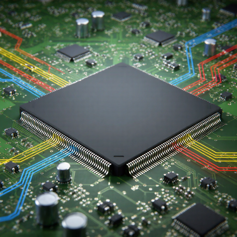
Table of Contents [Hide]
FPGA Basics: Definition, Purpose, and Core Characteristics
What Is an FPGA Chip and How Does It Work?
An FPGA, or field-programmable gate array, is a digital chip that users can configure after manufacturing. Unlike a fixed processor, it does not follow one permanent hardware path. Its internal fabric contains logic blocks, flip-flops, memory elements, and programmable routing channels. Engineers connect these resources to create circuits for specific tasks.
The purpose of an FPGA is flexible hardware acceleration. It can process several operations in parallel, often with predictable timing. A camera system might use it to filter pixels as they arrive. A control device could respond to sensor changes within carefully measured delays. Engineers usually describe the circuit with a hardware language, simulate its behavior, and then load the configuration into the chip. Timing still matters.
Core characteristics include reconfigurability, parallel execution, and direct control over data movement. Many devices also provide high-speed input connections, embedded memory, and arithmetic blocks. In practical development, I would inspect signal timing with test equipment and compare results against simulation. Small design errors can produce unstable outputs. That part is easy to underestimate. A circuit may work during a short test, then fail when temperature, clock speed, or input activity changes. Reliable FPGA work therefore depends on clear requirements, repeatable tests, and careful review of power and timing limits. A faster circuit is not always a better circuit.